
Optical Transceivers for AI Data Centers: Why Photonics Matters Now
Optical transceivers—compact modules that convert light-based signals from fiber or laser into electrical signals—are a foundational component of modern AI data centers. As organizations build ever-larger GPU clusters to train and serve generative AI models, the demands on interconnect bandwidth, latency and power efficiency have intensified. Emerging companies founded by engineers with hyperscale and satellite networking backgrounds are targeting mass production of transceivers to meet this surge in demand, aiming to shift more of the global supply chain toward locally manufactured, automated production.
What are optical transceivers and why do they matter for AI data centers?
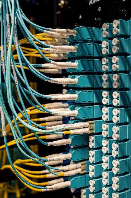
Optical transceivers enable high-speed communication between servers, switches and GPU enclosures by converting optical signals into electrical form and vice versa. For AI workloads—where tens of thousands of GPUs must exchange model parameters and gradients—the interconnect layer is as critical as raw compute. Efficient, high-density optical interconnects allow multiple GPUs to operate as a single, synchronized cluster, directly impacting training time, operational costs and power consumption.
Key functions of optical transceivers
- Convert optical signals from fiber or laser sources to electrical signals for switches and compute nodes.
- Support multi-terabit-per-second links with low latency suitable for distributed training.
- Enable dense cabling and modular rack architectures that save space and power.
How do photonic interconnects improve GPU cluster performance?
Photonic interconnects offer higher bandwidth-per-watt compared with many electrical interconnect solutions. For GPU clusters, that translates into fewer bottlenecks for parameter synchronization and faster iteration cycles during training. A small improvement in per-link efficiency compounds across thousands of links, producing meaningful savings in energy, cooling and total cost of ownership.
Performance advantages
- Lower latency across long-distance rack-to-rack links.
- Higher throughput enabling more scalable model parallelism.
- Reduced electromagnetic interference and improved signal integrity.
Why is domestic manufacturing of optical transceivers strategically important?
Today the market for optical transceivers is concentrated in a handful of regions. For AI-critical infrastructure, reliance on distant suppliers introduces supply-chain risk, lead-time variability and potential geopolitical exposure. Building domestic capacity for optical transceivers addresses several priorities:
- Reduced geopolitical risk and improved supply-chain resilience for hyperscalers and cloud providers.
- Closer integration between design teams and production lines, enabling faster iteration and tighter quality control.
- Potential national-security benefits when critical AI infrastructure depends on reliable, auditable components.
In parallel, investors and policymakers are increasingly viewing semiconductor and photonics supply chains through a strategic lens. For companies building next-generation AI systems, diversifying where components are produced is now a business and policy imperative.
What are the main challenges in scaling U.S.-based transceiver manufacturing?
Shifting high-volume optical module production to the U.S. presents technical, operational and ecosystem hurdles. Founders and engineers working to localize production frequently cite:
- Automation and lights-out manufacturing expertise: Many established high-speed optical assembly lines today rely on specialized, automated processes concentrated in other regions.
- Supply-chain onboarding: Equipment vendors, packaging suppliers and test labs must be aligned to support rapid qualification cycles for data-center customers.
- Capital intensity: Tooling, clean-room capacity and contract manufacturing setups require meaningful upfront investment to reach costs competitive with incumbents.
To overcome these barriers, startups are pursuing co-located design and production strategies, investing in automation and refining test-and-qualification processes to hit hyperscaler procurement standards.
How can removing power-hungry components reduce operational costs?
Design optimizations that remove or replace power-hungry components in transceivers can have outsized effects at scale. Even modest per-link power reductions—on the order of a few percent—compound across millions of links in hyperscale data centers and can reduce cooling loads as well as electricity costs. For example, a transceiver redesign that lowers per-cluster power draw by 3%–5% directly improves the efficiency of large GPU farms that already pursue aggressive performance-per-watt targets.
Why marginal gains matter
- Energy savings scale linearly with the number of links in a cluster.
- Smaller cooling requirements reduce facility CAPEX and OPEX.
- Power-efficient optics enable denser rack architectures and reduce space premiums.
What is the market opportunity for high-volume optical transceivers?
The transition to larger AI models and multi-exabyte data sets fuels demand for more advanced interconnects. Hyperscalers and cloud providers place large, repeatable orders once components reach qualification and cost thresholds. A company that can reliably manufacture thousands of transceivers per day while meeting performance and reliability specifications stands to capture significant share of a multi-billion-dollar market.
Key demand drivers include:
- Massive GPU clusters for training and inference.
- Expansion of regional AI data centers and edge facilities.
- Adoption of photonic fabrics inside rack and board-level interconnects.
Roadmap to volume production: what does it take?
Bringing optical transceivers to volume production involves a staged approach:
- Prototype and validation: design, lab testing, and interoperability checks with leading switches and NICs.
- Pilot manufacturing: small-batch production to refine yields and qualification procedures.
- Automation scale-up: invest in lights-out assembly lines, test automation and inline quality-control tools.
- Hyperscaler qualification: meet vendor acceptance for bulk orders and long-term supply agreements.
Companies targeting large customers often set aggressive throughput targets (for example, targeting the ability to produce thousands of units per day) to ensure they can support multi-year, multi-site deployment plans.
How will this change the economics and architecture of AI infrastructure?
Widespread availability of higher-performance, lower-power optical transceivers can reshape AI infrastructure economics in several ways:
- Lower network cost per GPU, making larger clusters economically viable.
- Faster training cycles, enabling faster model iteration and lower time-to-insight.
- New rack architectures that place greater emphasis on photonic backplanes and reduced electrical cabling complexity.
These effects combine to accelerate adoption of ever-larger models while allowing data-center operators to manage TCO more predictably.
How are investors and industry leaders responding?
Venture and growth investors are increasing bets on companies that can manufacture critical AI hardware components at scale, especially when those companies can present credible plans for automation and supply-chain diversification. Strategic investors see value in onshoring key components that power national and commercial AI infrastructure.
For readers interested in the broader capex and infrastructure dynamics influencing these investments, see our coverage of AI data-center spending and how megacapex bets are shaping the market: AI Data Center Spending: Are Mega-Capex Bets Winning?. For context on how chip and hardware automation is evolving, read AI Chip Design Automation: Ricursive Accelerates Hardware.
What are the broader implications for supply chains and policy?
Scaling domestic manufacturing of optical modules intersects with industrial policy, national security and commercial procurement. Policymakers seeking resilient AI infrastructure may favor incentives and incentives (tax credits, grants, procurement preferences) that accelerate capacity building locally. From a commercial standpoint, buyers increasingly demand predictable lead times, auditable supply chains and components that meet both performance and regulatory requirements.
Policy and procurement considerations
- Incentivize capital investment in automation and clean-room facilities.
- Standardize qualification processes so hyperscalers can onboard new suppliers faster.
- Encourage collaboration between design teams and domestic contract manufacturers.
What should data center operators and AI teams do now?
If you operate AI infrastructure or design distributed training systems, consider these practical steps:
- Audit your interconnect risk: map supplier geographies, lead times and single points of failure.
- Engage early with emerging transceiver suppliers to establish pilot agreements and test fixtures.
- Factor photonic options into next-generation cluster designs to evaluate power and latency trade-offs.
- Monitor qualification milestones and reserve capacity where possible to hedge supply risk.
Conclusion: photonics is a strategic lever for scaling AI
Optical transceivers and photonic interconnects are not just technical upgrades; they are strategic enablers for the next wave of AI infrastructure. By investing in automated, local manufacturing and production-scale expertise, companies can reduce supply-chain risk, improve performance-per-watt and help hyperscalers scale GPU clusters more economically. The industry is at an inflection point: the teams that can bridge high-performance photonic design with lights-out manufacturing will help define the interconnect stack for the next generation of large-scale AI.
Want to stay updated on AI infrastructure trends and hardware supply-chain shifts? Read our in-depth analysis of AI infrastructure investments and where capex is flowing: AI Infrastructure Investment in India: $200B Push.
Next steps (CTA)
If you manage AI infrastructure or invest in hardware supply chains, now is the time to evaluate photonic interconnect strategies. Contact our editorial team for introductions to startups in this space, subscribe for weekly analysis on AI infrastructure, or download our briefing on qualifying optical transceivers for GPU clusters.
Subscribe to Artificial Intel News for timely insights into AI hardware, data-center strategy and photonics innovations that will shape the next decade of AI.